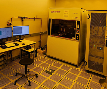
Nanofabrication Facilities:
We are equipped with two micro-nanofabrication facilities at UCF with the following capabilities-
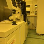
Lithography
Raith (Leica)EBPG 5000+
MJB4 UV Mask Aligner
MJB3 UV Mask Aligner
Mask Aligner & UV Lithography

Laser Lithography
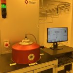
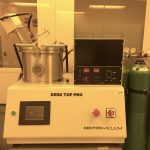
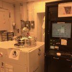
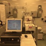
Deposition
Plasma-therm PECVD
Denton Pro Desktop Sputterer
Temescal Ebeam Evaporator
V&N Ebeam Evaporator
Bell jar Thermal Evaporator
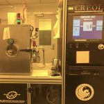
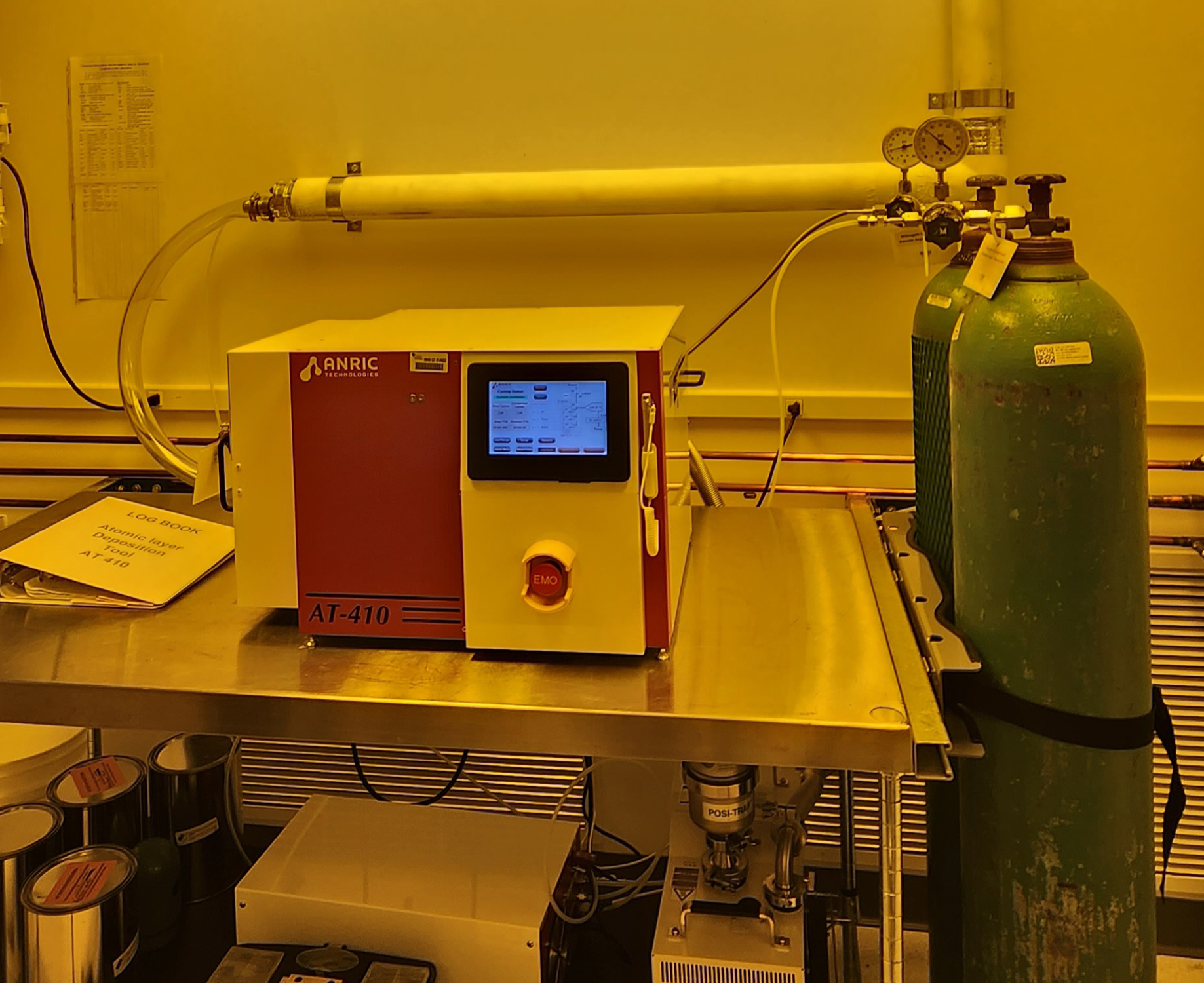
ALD System
6-Gun Sputtering System
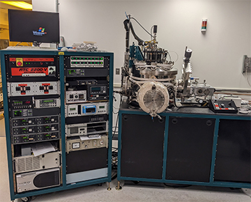
2-Gun EBeam Evaporation
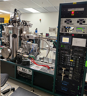
3-Gun Sputtering System

4-Gun Sputtering System
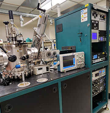
PECVD
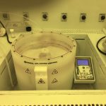
Spin coater
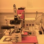
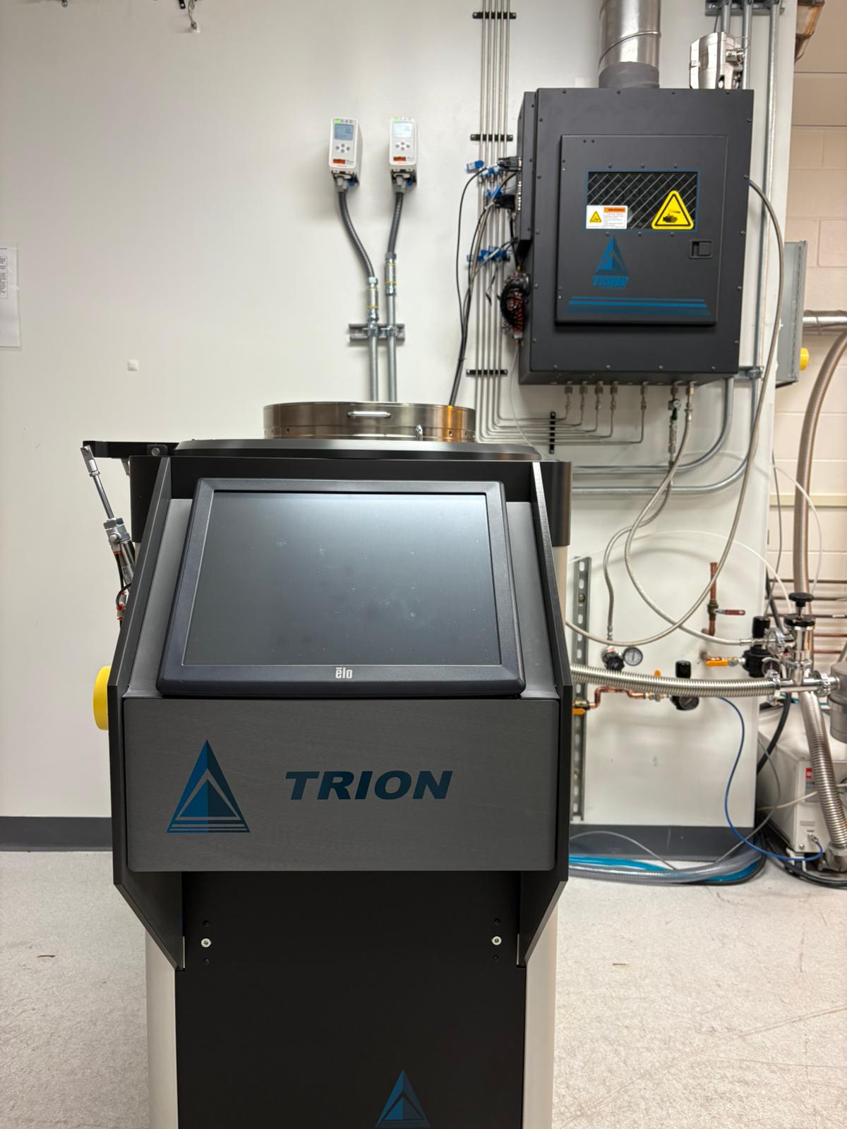
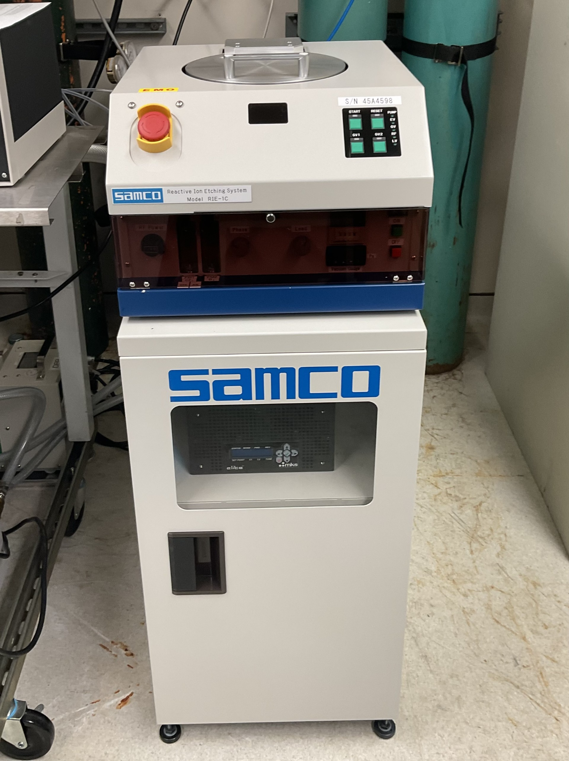
Etching
Takachi (formerly Apex) etcher
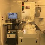
Oxford Plasma Pro 100
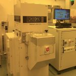
III-V Unaxis Shuttleline etcher
Tabletop RIE

RIE
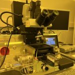
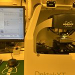
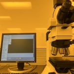
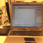
Material and Device Characterization in Cleanroom and MCF, UCF
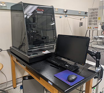
AFM
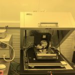
Profilometer
Nikon Optical Microscope
Filmetrics
Surface Profiler
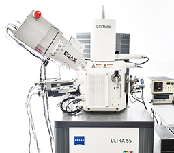
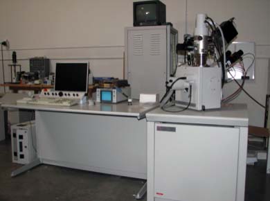
Scanning Electron Microscope

Zeiss ULTRA-55 FEG SEM (Scanning Electron Microscopy)
-Resolution 1 nm @ 15 KV, 1.7 nm @ 1 KV
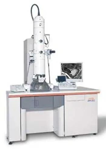
JEOL JSM-6480 SEM (Scanning Electron Microscopy)
-Accelerating Voltage: 0.3 to 30 kV
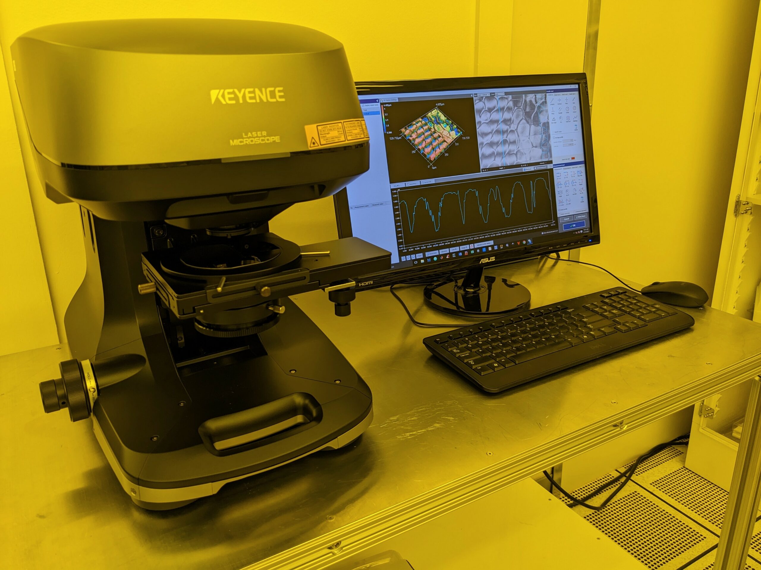
3-D Surface Profiler
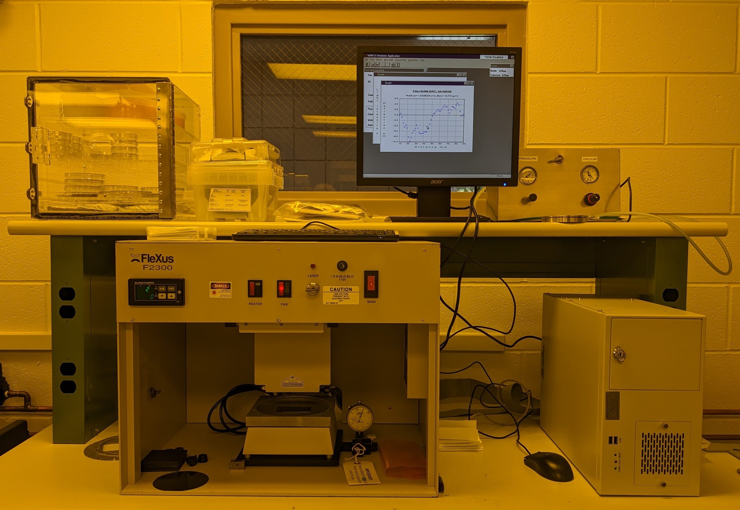
Thin Film Stress Measurement Tool
Focused Ion Beam
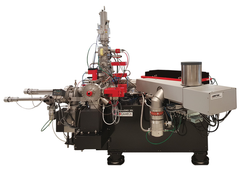
Cameca IMS-3F SIMS Ion Microscope
(Secondary Ion Mass Spectrometry)
-Primary ions: O2+, O-, Ar+, Xe+, Cs+ from 5 to 15kV
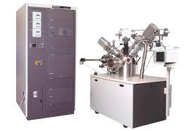
PHI Adept 1010 Dynamic SIMS System
(Secondary Ion Mass Spectrometry)
-Primary ions: O2+, Ar+, Xe+, Cs+ from 250eV to 8kV
Q-Lab Characterization Facilities: