Printed Circuit Board
PCB
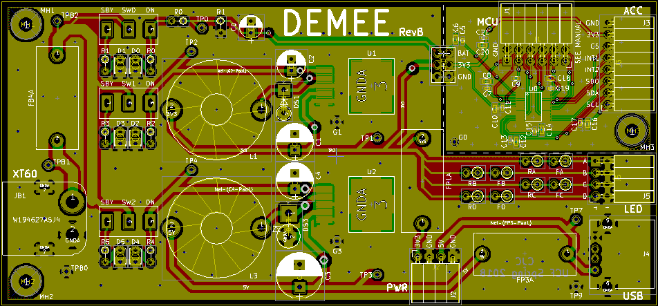
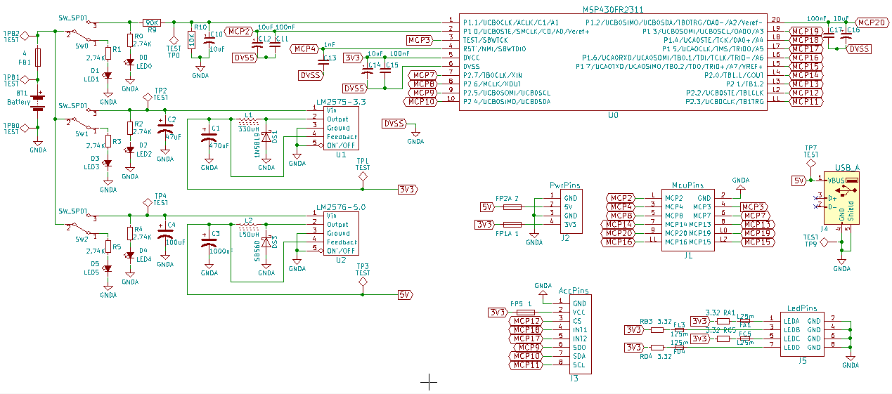
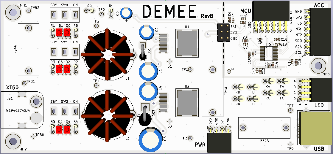
As can be seen in the figure above, battery power is applied at the XT60 connector on the left side of the board and is run through a 4 amp glass fuse for protection before terminating as a 29.6 volt rail for use by the board’s circuits. To the immediate right of this rail are three SPDT slide switches, along with red (standby) and green (on) status LEDs and their necessary resistors. The battery monitoring circuit, seen at the top of the layout, uses two resistors for voltage division and a 10 microFarad capacitor for noise filtering before terminating as an accessible pin at the edge of the power section’s ground plane. Just below the battery monitoring circuit is the 3.3 volt regulator circuit. This circuit contains the LM2575-3.3WU regulator previously mentioned, along with the necessary external components. Following the output trace of this circuit reveals three branches. One branch terminates as an accessible pin at the edge of the power section’s ground plane, another takes power to external pins for use with the experimental chamber LEDs, and the third takes power to an external header as a spare 3.3 volt connection. Below the 3.3 volt regulator circuit is the 5 volt regulator circuit. Similarly, this circuit contains the LM2576-5.0WU regulator and the necessary external components. The output trace from this circuit takes power to the USB port to power the Raspberry Pi, and to the PWR header as a spare 5 volt connection. At the top-right corner of the layout, one can see the microcontroller section of the board, shown with a dashed line. In this area of the board are the surfacemounted microcontroller, it’s decoupling capacitors, and its traces that terminate in female headers for use with the accelerometer and Raspberry Pi. This section has a separate ground plane from the power section of the board. These two ground planes are joined at a single point, with a jumper connection. This was done in an attempt to keep noise from the switching regulators away from the microcontroller traces.