Objectives
The ultimate goal of the project is to design a circuit that implements a specific time delay in the process of turning on a light emitting diode (LED).
Tools
- Circuit Simulator
- Lab Equipment
I. Circuit Network
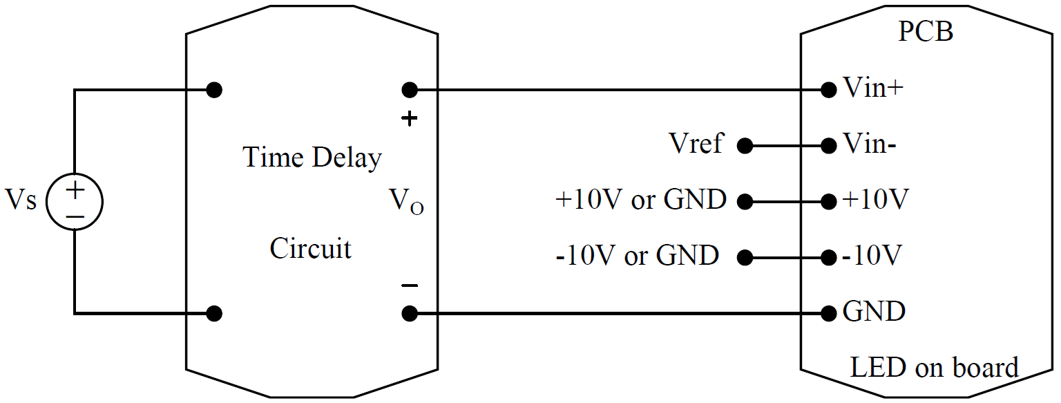
Figure 1 Circuit Network of Interest
As shown in Figure 1, the circuit network considered in this project has three major parts: DC voltage source (Vs), time delay circuit (TDC) and printed circuit board (PCB). The connections required to integrate the three parts are as follows:
- Input terminals of TDC are connected to Vs.
- Output terminals of TDC are connected to Vin+ and ground (GND) of PCB.
- Vin- of PCB is connected to Vref, which is a DC voltage with a specific value.
- +10V of PCB is connected to a +10V DC voltage or GND.
- -10V of PCB is connected to a -10V DC voltage or GND.
On the printed circuit board (PCB), there are two LEDs: green and red. The conditions for turning on these two LEDs are as follows:
- Green LED: Vin+ ≥ Vin- and +10V of PCB is connected to a +10V DC voltage
- Red LED: Vin- ≥ Vin+ and -10V of PCB is connected to a -10V DC voltage
II. Network Functionality
The circuit network in Figure 1 can be used to perform several functions. They include, but not limited to, the following:
- turn on the green LED after a specific time delay, td, for a given Vref value
- turn on the red LED after a specific time delay, td, for a given Vref value
- turn on both LEDs alternately with specific time intervals
For the current project, the focus will be on Function #1. Students are highly encouraged to work on implementing the remaining functions at their leisure.
III. The Challenge
Given the following items:
- a PCB with a red LED and a green LED on board
- a specified value for Vref
- a desired time delay value, td
the challenge is to perform all necessary steps such that the green LED will turn on only after the DC voltage source, Vs, has been turned on for a time duration specified by td. A successful challenge completion is demonstrated in the following video.
Video 1 A Successful Challenge Completion
To successfully tackle the challenge, complete the following tasks.
- Design the TDC.
- Determine the required value for Vs.
- Construct the circuit network in Figure 1 using the provided PCB. In addition to all other required connections, make the following connections:
- +10V of PCB to a +10V DC voltage
- -10V of PCB to GND
- Demonstrate to your ULAs that the green LED on the provided PCB can indeed be turned on only after the specified time duration has elapsed.
- Perform Step #4 three times and record down all 3 time delays using a timer.
- All 3 measured time delay values must fall within ±20% of the specified value td. You can exclude the adverse effect of human response time.
TECHNICAL NOTES:
- All node voltages, including Vin+, Vin-, +10V, and -10V of PCB, are defined with respect to the ground (GND). You should have this basic principle ingrained in your brain by now………
- WARNING: Make sure that the input values for both Vin+ and Vin- DO NOT exceed ±12V. Otherwise, circuit components on the PCB could be damaged.
IV. Assessment
The overall weighted grading scheme is as follows:
Table 1 Overall Weighted Grading Scheme
| Category | Percent of Overall Grade |
|---|---|
| Design Analysis (Simulation & Hand Analysis) | 30% |
| Implementation (No Partial Credit) | 40% |
| Report | 30% |
IMPORTANT NOTES:
- In the real world, your client will only accept an end product that is fully functional as specified or reject a failed product outright. Hence, the 40% score for implementation will be awarded based on all-or-nothing basis. To earn the full 40% score, all 3 measured time delay values must fall within ±20% of the specified value td.
- DO NOT blindly play around with component values using a circuit simulator in the hope that you will discover a working design. Even if you somehow manage to discover a working design magically, you will still lose substantial points in this project since you won’t be able to dissect your circuit design in your report using circuit theory, calculations, etc.
- All project demonstrations must be performed during a lab session. No project demonstration can be performed outside lab session.
- HEADS UP: Completing all the required tasks in this project requires substantial effort and time. To prepare fully for your project execution and demonstration, you are highly encouraged to complete the design analysis at home.
V. Report
Document all your analysis, results and findings in a report. The content of your report should include, but not limited to, the following sections.
- Objectives and Tasks – define and outline explicitly the objectives and tasks
- Dissection of Design – present your circuit design in a detailed, part-by-part analysis
– explain the reasonings behind your circuit design using circuit theory– provide detailed circuit analysis and calculation to justify the circuit topology,component type and component value used in your design
- Simulation Results – present your simulation results with clarity
– include screenshots of simulated circuits, results, etc.
- Experimental Results – present your experimental results with clarity
- Results Comparison – compare simulation and experimental results
– explain discrepancies pertaining to concepts
- Conclusions
The weighted grading scheme is as follows:
Table 2 Weighted Grading Scheme for Report
| Category | Percent of Overall Grade |
|---|---|
| Objectives and Tasks | 2.5% |
| Dissection of Design | 15.0% |
| Simulation Results | 2.5% |
| Experimental Results | 2.5% |
| Results Comparison | 5.0% |
| Conclusions | 2.5% |
| Total | 30% |