Objectives
- To analyze a resistive circuit using node or mesh analysis.
- To understand Thevenin’s and Norton’s theorems.
- To verify the superposition principle.
Equipment
- Breadboard
- DC power supply
- Digital multimeter (DMM)
Background
Electrical circuit analysis is the process of finding the voltages across and the currents through every component in the network. A number of techniques are frequently used for resistive circuits.
Nodal analysis is a method of determining the voltage at the nodes in an electrical circuit with respect to a reference node, using Kirchoff’s current law. Mesh analysis is a method that is used to solve for the current through any component in a planar circuit using Kirchoff’s voltage law. In some cases one method is clearly preferred over another. For example, when the circuit contains only voltage sources (or current sources), it is probably easier to use mesh analysis (or node analysis). It is often helpful to consider which method is more appropriate for the problem solution and make the selection.
Thevenin’s theorem, also called Thevenin equivalent, states that if we identify a pair of terminals in any circuit made up of both independent and dependent sources and resistors, the circuit can be replaced by an independent voltage source Voc in series with a resistor Rt. This series combination of Voc, the Thevenin voltage, and Rt, the Thevenin resistance, is equivalent to the original circuit in the sense that if we connect a same load across the terminals, we would get the same voltage and current at the terminals of the load as we would have with the original circuit. This equivalence holds for all possible values of load resistances. Voc is the open-circuit voltage of the original circuit across the terminals. Rt can be found by either of the two methods listed below. One is to find the short-circuit current isc, then find Rt using

The other method usually used in less complicated circuits involves deactivating the sources in the circuit, i.e. replacing all independent voltage sources with short circuits and all independent current sources with open circuits, and finding the equivalent resistance, which is Rt. Dependent current and voltage sources are not replaced with open circuits or short circuits.
Norton’s theorem, also referred as Norton equivalent, is a dual of Thevenin’s theorem. If we identify a pair of terminals in any circuit made up of both independent and dependent sources and resistors, the circuit can be replaced by a parallel combination of an ideal current source isc and a conductance Gn, where isc is the short-circuit current at the terminals in the original circuit and Gn is the ratio of the short-circuit current to the open-circuit voltage at the terminals in the original circuit.
The four parameters Voc, Rt, isc and Gn are related by


For linear circuits containing two or more independent sources, the superposition principle can also be used for circuit analysis. The voltage across (or the current through) any element can be obtained by adding algebraically all the individual voltages (or currents) caused by each independent source acting alone, with all the other independent voltage sources replaced by short circuits and all the other independent current sources replaced by open circuits.
Preparation
Nodal & Mesh Analysis, Thevenin’s Theorem and Superposition
For the circuit in Figure 3 – 1, all 7 resistors have different resistance values. For each resistor, choose any resistance value within the range of 1 kΩ to 56 kΩ unless specified otherwise. Refer to APPENDIX II for available resistors.
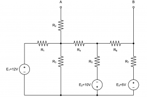
Figure 3-1 Circuit
- Short AB, as shown in Figure 3 – 2 (a). Use mesh analysis to calculate the voltage across each resistor and the current through AB, IAB.
- Leave AB open, as shown in Figure 3 – 2 (b). Use nodal analysis to calculate the voltage across each resistor as well as the voltage across AB, VAB.
- Find Thevenin’s and Norton’s Equivalent using the results from the previous two steps.
- Connect a resistor between nodes A and B. Use Thevenin’s theorem to calculate the current through this resistor for the following 3 resistor values: 1 kΩ, 2.2 kΩ and 4.7 kΩ.
- Leave AB open. Find the voltage across AB, VAB for the following 3 cases:
- E1 is turned on while both E2 and E3 are turned off;
- E2 is turned on while both E1 and E3 are turned off;
- E3 is turned on while both E1 and E2 are turned off.
Add the above three voltages. What have you discovered? Provide a detailed explanation of your discovery.
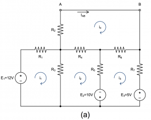
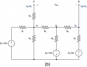
Figure 3 – 2 Mesh and nodal analysis. (a) mesh analysis; (b) nodal analysis
Simulation
Perform the following circuit simulations using a circuit simulator.
- Simulate the circuit in Figure 3 – 2 (a).
- Simulate the circuit in Figure 3 – 2 (b).
- With a resistor connected between nodes A and B, simulate the circuit for the following 3 resistor values: 1 kΩ, 2.2 kΩ and 4.7 kΩ.
- Simulate the circuit in Figure 3 – 2 (b) for the following 3 cases:
- E1 is turned on while both E2 and E3 are turned off;
- E2 is turned on while both E1 and E3 are turned off;
- E3 is turned on while both E1 and E2 are turned off.
Compare all the simulation results with those determined in PREPARATION.
Experiment
Build the circuit in Figure 3 – 1 on the breadboard. Refer to Section III in Experiment #1 to set the voltages sources in the circuit.
A. Mesh Analysis and Nodal Analysis
- Short AB by connecting a wire across nodes A and B. Measure the voltage across each resistor and the current through AB, IAB. Refer to the BACKGROUND section in Experiment #1 for how to use DMM to read the voltage and current values.
- Leave AB open. Measure the voltage across each resistor as well as the voltage across AB, VAB.
- Compare the results from step 1 and 2 with those obtained from PREPARATION and SIMULATION sections.
B. Thevenin’s and Norton’s Theorems
- Set all voltage sources to zero by simply replacing them with wires. With AB open, measure the resistance between AB using DMM. What resistance value are you measuring here? How does this measured value compare to the values obtained earlier in the PREPARATION and SIMULATION?
- Connect all voltages sources back into the circuit. With a resistor connected between A and B, measure the current through this resistor using DMM for the following 3 resistor values:
- 1 kΩ,
- 2.2 kΩ,
- 4.7 kΩ.
How do these current values compare to those obtained in the PREPARATION and SIMULATION.
C. Superposition Principle
- With AB open, measure the voltage across AB, VAB for the following 3 cases:
- E1 is turned on while both E2 and E3 are turned off;
- E2 is turned on while both E1 and E3 are turned off;
- E3 is turned on while both E1 and E2 are turned off.
Add the above three voltages. What have you discovered? Compare the results with those obtained in PREPARATION and SIMULATION.
- With AB open, measure the voltage across AB, VAB for the following 2 cases:
- E1 is turned on while both E2 and E3 are turned off;
- both E2 and E3 are turned on while E1 is turned off.
Add the above two voltages. What have you discovered? Provide a detailed explanation of your discovery.
- With AB open, measure the voltage across AB, VAB for the following 3 cases:
- both E1 and E2 are turned on while E3 is turned off;
- both E1 and E3 are turned on while E2 is turned off;
- both E2 and E3 are turned on while E1 is turned off.
Add the above three voltages. What have you discovered? Provide a detailed explanation of your discovery.