Objectives
- To study the step response of first order circuits.
- To understand the concept of the time constant.
- To study the step response of second order circuits.
- To understand the difference between overdamped, critically damped and underdamped responses.
- To determine theoretically and experimentally the damped natural frequency in the under-damped case.
Equipment
- Breadboard
- Function generator
- Oscilloscope
- Digital multimeter (DMM)
Background
A. First Order Circuits
First-order transient circuits are described by a first order differential equation. First-order circuits contain a resistor and only one type of storage element, either an inductor or a capacitor, i.e. RL or RC circuits.
For a step voltage/current source input, the output can be expressed as
![X(t)=X(\infty)+[X(0)-X(\infty)] \times e^{-{t \over \tau}}](https://www.ece.ucf.edu/labs/EEL3123/wp-content/ql-cache/quicklatex.com-80215ae2a1a4d513185a69df0995ee06_l3.png "Rendered by QuickLaTeX.com")
Where,  is the circuit response at
  , and
, and  is the response at
  . The parameter
  is called time constant of the circuit and gives the time required for the response (i) to rise from zero to 63% (or
  ) of its final steady value as shown in Figure 4 – 1 (a), or (ii) to fall to 37% (or
  ) of its initial value as shown in Figure 4 – 1 (b). Therefore, the smaller the value of , the faster the circuit response is.
For a RC circuit
\color{black}\tau = R \times C
For a RL circuit
\color{black}\tau = {L \over R}
Applying the equations above, the voltage responses across the capacitor and the resistor in Figure 4-1 can be written as:


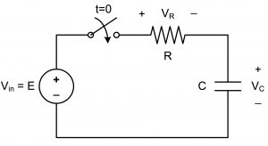
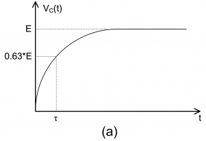
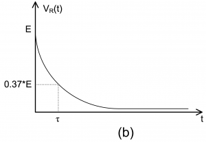
Figure 4 – 1 A first order circuit and its responses. (a) voltage over the capacitor; (b) voltage over the resistor.
B. Second Order Circuits
Second-order circuits are RLC circuits that contain two energy storage elements. They can be represented by a second-order differential equation. A characteristic equation, which is derived from the governing differential equation, is often used to determine the natural response of the circuit. The characteristic equation usually takes the form of a quadratic equation, and it has two roots s1 and s2.


When these roots are rewritten as,


then the natural response of the circuit is determined by:
 , there are two real and distinct roots
  Overdamped, as shown in Figure 4 – 2 (a) and (d).
 , there are two real equal roots Critically damped, as shown in Figure 4 – 2 (b) and (e).
 , there are two complex roots Underdamped, as shown in Figure 4 – 2 (c) and (f).
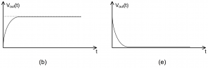
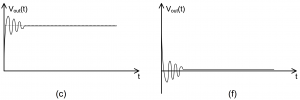
Figure 4 – 2 Second order circuits natural responses
Preparation
A. First Order Circuits
Figure 4 – 3 and Figure 4 – 4 show various RC and RL circuits. For all circuits, R = 1 kΩ, C = 0.1 uF, and L = 100 mH.
- For the circuits in Figure 4 – 3, derive the analytical expression for
 given that \color{black}E is a constant. Sketch or plot for each circuit.
 - For the circuits in Figure 4 – 4, \color{black}V_{in}(t) is a symmetric square wave input with amplitude
 and period
  . Sketch or plot for each circuit using superposition and the hint below. Show at least three cycles.
 - For the circuit in Figure 4 – 4 (d), with \color{black}V_{in}(t) remains unchanged, sketch or plot the voltage across the inductor. Show at least three cycles. Compare this voltage waveform to the one obtained from the circuit in Figure 4 – 4 (c). What do you observe? Why?
Hint: the square wave can be broken up into a series of step voltage waveforms with alternating polarities. Each of these step voltage inputs generates an output, and the total output response is the summation of all the individual outputs.
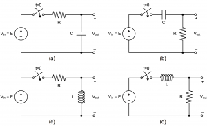
Figure 4 – 3 First order circuits with step input voltage
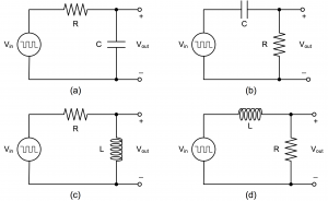
Figure 4 – 4 First order circuits with square wave input
B. Second Order Circuits
Figure 4 – 5 and Figure 4 – 6 show various 2nd order circuits. For all circuits, C = 0.01 uF and L = 100 mH.
- For both circuits in Figure 4 – 5, \color{black}E is a constant. Write down the characteristic equation. Also, calculate the resistance range for R for the following cases.
- Over-damped response
- Critically damped response
- Under-damped response
- For the circuit in Figure 4 – 5 (a), plot or sketch the response when the resistor has the following resistance values.
- R = 22 kΩ
- R = 6.3 kΩ
- R = 2.2 kΩ
- For the circuit in Figure 4 – 5 (b), plot or sketch the response when the resistor has the following resistance values.
- R = 680 Ω
- R = 1.6 kΩ
- R = 4.7 kΩ
- For both circuits in Figure 4 – 6, \color{black}V_{in}(t) is a symmetric square wave input with a frequency of 400 Hz and an amplitude of 4 V. Set R = 470 Ω for the circuit in Figure 4 – 6 (a) and R = 22 kΩ for the circuit in Figure 4 – 6 (b).
- Calculate α, ωo, and ωd.
- Plot or sketch the output voltage, .
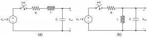
Figure 4 – 5 Second order circuits with step input voltage

Figure 4 – 6 Second order circuits with square wave input
Simulation
Perform the following circuit simulations using a circuit simulator.
- Build and simulate the circuits in Figure 4 – 4. Set the input voltage to
 with a frequency of 1 kHz. Display both
  and on the oscilloscope. Compare the results with the plots from PREPARATION.
 - For the circuit in Figure 4 – 4 (d), with the input voltage remains unchanged, display the voltage across the inductor. Compare this voltage waveform to the one obtained from the circuit in Figure 4 – 4 (c). What do you observe? Why?
- Build and simulate the circuits in Figure 4 – 6. Set the input voltage to
 with a frequency of 400 Hz. Display both and on the oscilloscope. Compare the results with the plots from PREPARATION.
First Order Circuits Experiment
Construct all four circuits in Figure 4 – 4. Use the same component values as in the PREPARATION and the same input settings used in the SIMULATION. Complete the measurements described below. Refer to Experiment #3 for instructions on how to use function generator and oscilloscope.
A. Response to square wave input
- Measure both the input and the output using the oscilloscope. Connect Ch1 to the input and Ch2 to the output so that both waveforms are displayed on the screen. Compare these waveforms to the results from PREPARATION and SIMULATION.
- For the circuit in Figure 4 – 4 (d), measure the voltage across the inductor using the oscilloscope. Since any voltage measured by the probe used in the lab is with respect to the ground, the voltage across the inductor has to be measured indirectly. This measurement can be obtained using the ‘Math’ button on the oscilloscope. Compare this voltage waveform to the one obtained from the circuit in Figure 4 – 4 (c). What do you observe? Why?
- Save the screen images to a USB drive using the ‘Save Load’ button.
B. Time constant measurement
- Turn off the input (Channel 1) by pressing the channel number button. Now only the output is displayed on the screen.
- Zoom in on the output curve on the oscilloscope such that a large portion (at least half a cycle) of the rise/drop of a cycle is displayed on the screen. Consider the rise and drop over one half cycle only for each circuit. Use cursors to determine the maximum voltage difference E for the output. The time it takes for the output to rise from the minimum value to 63% of E or to drop from the maximum to 37% of E is the time constant of the circuit. Record this time constant for each circuit.
Second Order Circuits Experiment
On the function generator use the same square wave input settings as in SIMULATION. Build both circuits shown in Figure 4 – 6.
A. Natural responses
- Measure the output voltage for the following six cases.
- R = 22 kΩ in the circuit of Figure 4 – 6 (a)
- R = 6.3 kΩ in the circuit of Figure 4 – 6 (a)
- R = 2.2 kΩ in the circuit of Figure 4 – 6 (a)
- R = 680 Ω in the circuit of Figure 4 – 6 (b)
- R = 1.6 kΩ in the circuit of Figure 4 – 6 (b)
- R = 4.7 kΩ in the circuit of Figure 4 – 6 (b)
- On the oscilloscope, connect Ch1 to the input and Ch2 to the output so that both the input and the output are displayed on the screen.
- For each case, save the screen image with the associated measurements for both the input and the output on to a USB drive.
- For each case, indicate if the output response is overdamped, critically damped or underdamped.
B. Damped natural frequency measurement
- Set R = 470 Ω for the circuit in Figure 4 – 6 (a) and R = 22 kΩ for the circuit in Figure 4 – 6 (b). Measure and save the screen image for both the input and the output, and compare them with the results from PREPARATION and SIMULATION.
- Zoom in on the output curve so that at least two whole oscillations (ripples) of the output from the beginning of an output cycle are displayed. Use the cursors to measure the time period Td between the first two peaks (or between two zero phases). ωd is calculated using:
